This document provides a detailed overview of the GNSS pinout configuration for INS hardware, offering clear and precise information about the purpose and functionality of each pin. Understanding the pinout is essential for establishing proper connections, ensuring reliable data communication, and achieving optimal performance in GNSS-enabled applications.
Engineers, technicians, and system integrators can seamlessly integrate INS hardware into their systems with this pinout description. Each pin’s role, signal type, and use case are outlined to support the device’s accurate setup and smooth operation in navigation and data acquisition environments.
Explore the specifics of the GNSS pinout configuration to unlock the full potential of your INS hardware and ensure seamless integration into your applications.
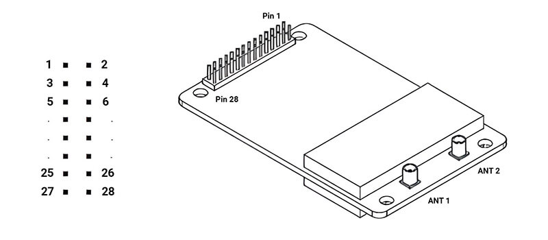
Pinout Description
| Pin | I/O | Description |
|---|---|---|
|
1 |
N/A |
Not used |
|
2 |
N/A |
Not used |
|
3 |
N/A |
Not used |
|
4 |
N/A |
Not used |
|
5 |
Power |
Antenna feed input |
|
6 |
Power |
Power input |
|
7 |
I |
SPI Data |
|
8 |
I |
COM3 input data |
|
9 |
I |
Reset input |
|
10 |
I |
Reset |
|
11 |
I |
Event |
|
12 |
I |
Reserve |
|
13 |
O |
COM3 output |
|
14 |
Power |
GND |
|
15 |
O |
COM1 output |
|
16 |
I |
COM1 input |
|
17 |
Power |
GND |
|
18 |
O |
COM2 output |
|
19 |
I |
COM2 input |
|
20 |
Power |
GND |
|
21 |
O |
Reserve |
|
22 |
Power |
GND |
|
23 |
O |
PPS |
|
24 |
I |
Reserve |
|
25 |
N/A |
Not used |
|
26 |
N/A |
Not used |
|
27 |
N/A |
Not used |
|
28 |
N/A |
Not used |